1. Material Fundamentals and Structural Features of Alumina Ceramics
1.1 Crystallographic and Compositional Basis of α-Alumina
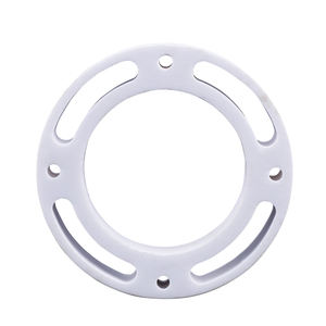
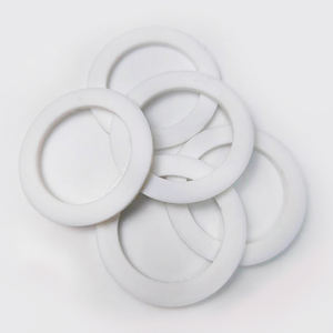
(Alumina Ceramic Substrates)
Alumina ceramic substrates, largely composed of light weight aluminum oxide (Al two O FOUR), serve as the foundation of contemporary digital product packaging as a result of their extraordinary equilibrium of electric insulation, thermal security, mechanical stamina, and manufacturability.
One of the most thermodynamically steady stage of alumina at high temperatures is corundum, or α-Al Two O FIVE, which takes shape in a hexagonal close-packed oxygen lattice with light weight aluminum ions inhabiting two-thirds of the octahedral interstitial sites.
This thick atomic setup imparts high hardness (Mohs 9), exceptional wear resistance, and solid chemical inertness, making α-alumina appropriate for extreme operating settings.
Business substrates commonly contain 90– 99.8% Al ₂ O SIX, with small enhancements of silica (SiO ₂), magnesia (MgO), or uncommon planet oxides utilized as sintering aids to promote densification and control grain growth throughout high-temperature processing.
Greater purity qualities (e.g., 99.5% and over) show remarkable electric resistivity and thermal conductivity, while lower pureness variations (90– 96%) use affordable services for much less requiring applications.
1.2 Microstructure and Flaw Design for Electronic Integrity
The performance of alumina substratums in electronic systems is critically dependent on microstructural uniformity and flaw reduction.
A penalty, equiaxed grain framework– typically varying from 1 to 10 micrometers– makes certain mechanical stability and lowers the likelihood of crack propagation under thermal or mechanical stress and anxiety.
Porosity, specifically interconnected or surface-connected pores, must be reduced as it degrades both mechanical stamina and dielectric performance.
Advanced handling techniques such as tape spreading, isostatic pushing, and controlled sintering in air or controlled ambiences allow the manufacturing of substratums with near-theoretical density (> 99.5%) and surface area roughness below 0.5 µm, essential for thin-film metallization and wire bonding.
In addition, pollutant partition at grain borders can cause leak currents or electrochemical movement under prejudice, necessitating stringent control over basic material pureness and sintering problems to make sure long-lasting reliability in humid or high-voltage environments.
2. Production Processes and Substrate Construction Technologies
( Alumina Ceramic Substrates)
2.1 Tape Casting and Eco-friendly Body Processing
The manufacturing of alumina ceramic substrates starts with the preparation of an extremely spread slurry consisting of submicron Al ₂ O six powder, organic binders, plasticizers, dispersants, and solvents.
This slurry is refined by means of tape spreading– a continual method where the suspension is topped a moving provider movie utilizing a precision doctor blade to accomplish consistent density, typically in between 0.1 mm and 1.0 mm.
After solvent evaporation, the resulting “eco-friendly tape” is flexible and can be punched, drilled, or laser-cut to form using openings for vertical affiliations.
Multiple layers might be laminated flooring to develop multilayer substrates for intricate circuit integration, although the majority of industrial applications use single-layer configurations due to cost and thermal growth considerations.
The environment-friendly tapes are then very carefully debound to eliminate natural ingredients with managed thermal disintegration prior to final sintering.
2.2 Sintering and Metallization for Circuit Assimilation
Sintering is conducted in air at temperature levels between 1550 ° C and 1650 ° C, where solid-state diffusion drives pore removal and grain coarsening to attain full densification.
The direct shrinking throughout sintering– typically 15– 20%– should be precisely anticipated and made up for in the design of eco-friendly tapes to make certain dimensional accuracy of the final substrate.
Following sintering, metallization is put on develop conductive traces, pads, and vias.
Two key methods control: thick-film printing and thin-film deposition.
In thick-film modern technology, pastes including steel powders (e.g., tungsten, molybdenum, or silver-palladium alloys) are screen-printed onto the substratum and co-fired in a minimizing atmosphere to develop robust, high-adhesion conductors.
For high-density or high-frequency applications, thin-film procedures such as sputtering or evaporation are made use of to deposit bond layers (e.g., titanium or chromium) followed by copper or gold, enabling sub-micron pattern through photolithography.
Vias are filled with conductive pastes and terminated to develop electric affiliations between layers in multilayer layouts.
3. Practical Qualities and Performance Metrics in Electronic Systems
3.1 Thermal and Electrical Actions Under Operational Stress And Anxiety
Alumina substratums are treasured for their beneficial mix of modest thermal conductivity (20– 35 W/m · K for 96– 99.8% Al Two O FOUR), which allows efficient warm dissipation from power devices, and high volume resistivity (> 10 ¹⁴ Ω · centimeters), guaranteeing very little leakage current.
Their dielectric consistent (εᵣ ≈ 9– 10 at 1 MHz) is secure over a broad temperature and frequency variety, making them ideal for high-frequency circuits up to a number of gigahertz, although lower-κ materials like light weight aluminum nitride are liked for mm-wave applications.
The coefficient of thermal expansion (CTE) of alumina (~ 6.8– 7.2 ppm/K) is fairly well-matched to that of silicon (~ 3 ppm/K) and certain packaging alloys, lowering thermo-mechanical anxiety throughout device operation and thermal cycling.
However, the CTE mismatch with silicon continues to be a problem in flip-chip and direct die-attach setups, frequently needing certified interposers or underfill products to minimize tiredness failing.
3.2 Mechanical Toughness and Environmental Sturdiness
Mechanically, alumina substrates show high flexural toughness (300– 400 MPa) and outstanding dimensional security under load, allowing their use in ruggedized electronics for aerospace, auto, and industrial control systems.
They are resistant to resonance, shock, and creep at raised temperatures, keeping structural stability approximately 1500 ° C in inert ambiences.
In humid environments, high-purity alumina reveals marginal dampness absorption and outstanding resistance to ion movement, making sure lasting integrity in outdoor and high-humidity applications.
Surface hardness additionally safeguards versus mechanical damage during handling and assembly, although treatment should be required to prevent side damaging as a result of integral brittleness.
4. Industrial Applications and Technical Influence Across Sectors
4.1 Power Electronics, RF Modules, and Automotive Solutions
Alumina ceramic substratums are ubiquitous in power electronic modules, including shielded gate bipolar transistors (IGBTs), MOSFETs, and rectifiers, where they provide electrical seclusion while facilitating warmth transfer to warm sinks.
In radio frequency (RF) and microwave circuits, they act as carrier systems for crossbreed integrated circuits (HICs), surface area acoustic wave (SAW) filters, and antenna feed networks as a result of their secure dielectric properties and reduced loss tangent.
In the automotive industry, alumina substrates are made use of in engine control systems (ECUs), sensor bundles, and electrical vehicle (EV) power converters, where they endure high temperatures, thermal cycling, and exposure to harsh liquids.
Their dependability under extreme problems makes them essential for safety-critical systems such as anti-lock braking (ABDOMINAL) and progressed driver aid systems (ADAS).
4.2 Clinical Devices, Aerospace, and Arising Micro-Electro-Mechanical Solutions
Past consumer and commercial electronic devices, alumina substrates are used in implantable medical gadgets such as pacemakers and neurostimulators, where hermetic securing and biocompatibility are paramount.
In aerospace and protection, they are made use of in avionics, radar systems, and satellite communication components as a result of their radiation resistance and stability in vacuum cleaner environments.
Furthermore, alumina is significantly made use of as a structural and insulating system in micro-electro-mechanical systems (MEMS), including pressure sensing units, accelerometers, and microfluidic tools, where its chemical inertness and compatibility with thin-film handling are helpful.
As digital systems remain to require greater power densities, miniaturization, and dependability under extreme problems, alumina ceramic substrates stay a keystone material, linking the space in between efficiency, expense, and manufacturability in advanced electronic product packaging.
5. Vendor
Alumina Technology Co., Ltd focus on the research and development, production and sales of aluminum oxide powder, aluminum oxide products, aluminum oxide crucible, etc., serving the electronics, ceramics, chemical and other industries. Since its establishment in 2005, the company has been committed to providing customers with the best products and services. If you are looking for high quality pure alumina, please feel free to contact us. (nanotrun@yahoo.com)
Tags: Alumina Ceramic Substrates, Alumina Ceramics, alumina
All articles and pictures are from the Internet. If there are any copyright issues, please contact us in time to delete.
Inquiry us